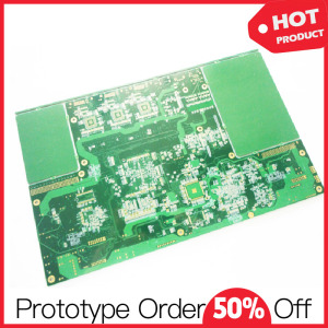

Smart Home Bell PCB Single Circuit Board
-
Price:
Negotiable
- minimum:
- Total supply:
-
Delivery term:
The date of payment from buyers deliver within days
-
seat:
Guangdong
-
Validity to:
Long-term effective
-
Last update:
2017-09-16 00:52
-
Browse the number:
188
+
Guangzhou NOD Electronics Co., Ltd.
- Contactaixin:
Mr. Rocky Long(Mr.)
-
Email:
telephone:
phone:

-
Arrea:
Guangdong
Address:Block3, #20-8, Huanxi West Rd, Tianhe District, Guangzhou, Guangdong, China 510660
- Website:
+
ROHS 94V0 Single Circuit Board with Quality Commitment
Products Description
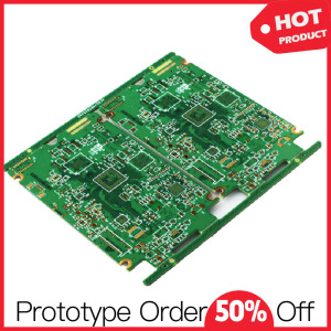
Single Circuit Board Manufacturing Capabilities
Our single circuit board manufacturing capabilities can meet almost 95% demand of customer requirements and actually we concentrated on this field for decades, so plant facilities have been advanced to high level and your intelligent manufacturing could be well handled here
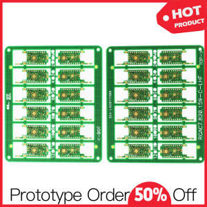
Single Circuit Board Assembly Manufacturing Capabilities
If bare PCB is bone, PCB assembly is flesh and blood. PCB manufacture assembly highly determines the total quality of PCBA functions. Our sophisticated engineers excute SOPs and weekly training to ensure the manufacturing processes. Advanced SMT lines can catch up with your demand of high-precision soldering, such as 0201, 0.25mm BGAs, PQFP, PLCC, SOP, SOJ etc. Now we have 6 SMT assembly lines and 4 DIP lines.
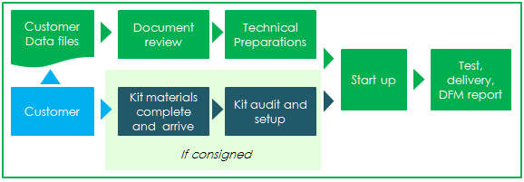
Single Circuit Board Manufacturing Process
About Us
As a service-leading PCB manufacturing and PCB assembly (PCBA) partner, NOD Electronics strives to support international small-medium business with 10+ years engineering experience in Electronic Manufacturing Services (EMS). Our headquarter is located in Guangzhou, China. We have 10,000 square meters plant, 287 employees and 42 engineers, monthly capabilities of 15,000 square meters PCB design & fabrication and 80 million spot SMT. We were approved by ISO9001-2008, TS16949, UL, CE, RoHS.
Our customers are widely distributed in mainland China, Taiwan, the United States, Japan, Singapore, Korea, Russia, Germany, Switzerland and other parts of the word.

Your single circuit board demand will be perfectly handled by our professional production line and responsible work team.
Frequently Asked Questions (FAQs)
How we ensure the quality of circuit board manufacturing and assembly?
We choose top sheet suppliers to ensure stable performance (general FR-4). During the manufacturing process, automatic copper plating lines and high-speed drilling machines (brand:TMAX) to make accuracy and fast delivery guaranteed. All printed circuit board will be detected by advanced automatic flying probe machines (or test frame ) at subsequent stages to make sure each PCB is OK from inner circuits to outside shape.
How long will you get our quotation of PCB manufacturing and assembly?
In general, PCB sample is delivered in 24~72 hours (urgent order less than 24 hours). Volume production can be completed in 7 working days. If for subsequent PCB assembly and test requirements, the lead time could be less than 15 days.
What kind of files you have to send us to get quotation?
You have to send us PCB design files (gerbers or .pcb acceptable), Bill of Materials (BOM), Quantities to make quote and other technical requirements (.step/.txt/.xls files acceptable)
What payment methods we can support?
We accept T/T, L/C, West Union as payment methods. For prototype order, you have to make 100% payment in advance, but for mass production 70% payment in advance and 30% payment before delivery.
What measures we take to avoid counterfeit components?
Procurement only from manufacturer or big general agent
Original quality certificate of component can be issued (if necessary)
Inspections of shape, silkscreen and conductivity attributes in incoming quality control
Strong responsibilities and perspectives of long-term relationship
What measures we take to protect clients IP and confidentiality?
Sign NDA (Non-disclosure Agreement)
Using number code in stead of client name during manufacturing process
Separate assembly workshop and taking photo is NOT allowed
Documents of engineering process are archived and reserved
Products Description
| Layer Count | 1 to 22 layer |
| Material Type | FR-4, CEM-1, CEM-3, High TG, FR4 Halogen Free, Rogers.etc. |
| Board Thickness | 0.21mm to 7.0mm |
| Copper Thickness | 0.5 oz to 7.0 oz |
| Min. Line Width&Space | 3/3 mil |
| Min. Mechnical Hole | 0.15mm(0.8mm for Alu PCB) |
| Min.Solder Mask Dam | 0.075mm |
| Max.Aspect Ratio | 10:01 |
| PTH Size Tolerance | +/- 0.05mm |
| Impedance Control Tolerance | +/- 8% |
| Routing Tolerance | +/- 0.1mm |
| Electric Strength | >103KV/mm |
| Current Breakdown | 10A |
| Solder Mask Abrasion | >6H |
| Solder Mask Color | Green/Black/White/Red/Blue/Matt Blue/Matt Black |
| Silkscreen Color | Yellow/Black/White/ Orange/Grey |
| Surface Finishing | HASL / HASL lead free,OSP, Tin Plating, Silver Plating Immersion Silver/Tin, ENIG, Hard Gold plating |
| PCB Packing | Inner Packing :Vacuum Packing /Plastic bag Outer Packing :Standard carton packing |
Single Circuit Board Manufacturing Capabilities
Our single circuit board manufacturing capabilities can meet almost 95% demand of customer requirements and actually we concentrated on this field for decades, so plant facilities have been advanced to high level and your intelligent manufacturing could be well handled here
| Total Pad Size | Standard | Advanced |
| Capture Pad | Drill + 0.008 | Drill + 0.006 |
| Landing Pad | Drill + 0.008 | Drill + 0.006 |
| BC Mechanical Drill (Type III) | 0.008 | 0.006 |
| Laser Drill Size | 0.004-0.010 | 0.0025 |
| Material Thickness | 0.0035 | 0.0025 |
| Stacked Via | Yes | Yes |
| Type I Capabilities single & Double Deep | Yes | Yes |
| Type II Capabilities Buried Vias with Microvias | Yes | Yes |
| Type III Capabilities | Yes | Yes |
| Copper Filled Microvia | Yes | Yes |
| Smallest Copper Filled Microvia | 0.004 | 0.0025 |
| Copper Filled Microvia Aspect Ratio | 0.75:1 | 1:01 |
| Smallest Laser Microvia Hole Size | 0.004 | 0.0025 |
| Laser Via Aspect Ratio (Depth:Diameter) | 0.75:1 | c |
Single Circuit Board Assembly Manufacturing Capabilities
If bare PCB is bone, PCB assembly is flesh and blood. PCB manufacture assembly highly determines the total quality of PCBA functions. Our sophisticated engineers excute SOPs and weekly training to ensure the manufacturing processes. Advanced SMT lines can catch up with your demand of high-precision soldering, such as 0201, 0.25mm BGAs, PQFP, PLCC, SOP, SOJ etc. Now we have 6 SMT assembly lines and 4 DIP lines.
| Turn Times | Selected Volume | Selected Solder Types |
| Same day through four weeks turns | No minimum order quantity | Leaded |
| Scheduled deliveries | Engineering prototypes | Lead-free/RoHS compliant |
| Low cost first article builds | No-clean process available | |
| Parts Procurement | Selected Stencils | Selected Ball Grid Arrays (BGA) |
| Turnkey | Laser cut stainless steel | As small as .5mm pitch |
| Kitted/Consigned | Nano-coating available | All BGA placements are x-ray inspected |
| Partial Turnkey | ||
| Assembly Types | Selected Component Types | Selected Other Capabilities |
| Surface Mount (SMT) | As small as 0402 package | Pitch components as small as 15 mil |
| Thru-hole | As small as 0201 with design review | Repair/Rework services |
| Mixed Technology (SMT/Thru-hole) | Mechanical Assembly | |
| Single or double sided placement | Box Build/Electromechanical Assembly | |
| Sub-assemblies |
Single Circuit Board Manufacturing Process
About Us
As a service-leading PCB manufacturing and PCB assembly (PCBA) partner, NOD Electronics strives to support international small-medium business with 10+ years engineering experience in Electronic Manufacturing Services (EMS). Our headquarter is located in Guangzhou, China. We have 10,000 square meters plant, 287 employees and 42 engineers, monthly capabilities of 15,000 square meters PCB design & fabrication and 80 million spot SMT. We were approved by ISO9001-2008, TS16949, UL, CE, RoHS.
Our customers are widely distributed in mainland China, Taiwan, the United States, Japan, Singapore, Korea, Russia, Germany, Switzerland and other parts of the word.
Your single circuit board demand will be perfectly handled by our professional production line and responsible work team.
Frequently Asked Questions (FAQs)
How we ensure the quality of circuit board manufacturing and assembly?
We choose top sheet suppliers to ensure stable performance (general FR-4). During the manufacturing process, automatic copper plating lines and high-speed drilling machines (brand:TMAX) to make accuracy and fast delivery guaranteed. All printed circuit board will be detected by advanced automatic flying probe machines (or test frame ) at subsequent stages to make sure each PCB is OK from inner circuits to outside shape.
How long will you get our quotation of PCB manufacturing and assembly?
In general, PCB sample is delivered in 24~72 hours (urgent order less than 24 hours). Volume production can be completed in 7 working days. If for subsequent PCB assembly and test requirements, the lead time could be less than 15 days.
What kind of files you have to send us to get quotation?
You have to send us PCB design files (gerbers or .pcb acceptable), Bill of Materials (BOM), Quantities to make quote and other technical requirements (.step/.txt/.xls files acceptable)
What payment methods we can support?
We accept T/T, L/C, West Union as payment methods. For prototype order, you have to make 100% payment in advance, but for mass production 70% payment in advance and 30% payment before delivery.
What measures we take to avoid counterfeit components?
Procurement only from manufacturer or big general agent
Original quality certificate of component can be issued (if necessary)
Inspections of shape, silkscreen and conductivity attributes in incoming quality control
Strong responsibilities and perspectives of long-term relationship
What measures we take to protect clients IP and confidentiality?
Sign NDA (Non-disclosure Agreement)
Using number code in stead of client name during manufacturing process
Separate assembly workshop and taking photo is NOT allowed
Documents of engineering process are archived and reserved